Laser annealing is one of the technologies used in the semiconductor manufacturing process. In recent years, as the realization of a decarbonized society has become more important, power semiconductors have been attracting attention, and laser annealing plays a role in their manufacturing process. This article introduces the features and benefits of laser annealing and the laser annealing process in power semiconductor manufacturing.
TECH INFORMAITON
Laser Annealing
Laser Annealing - Power Semiconductor Manufacturing
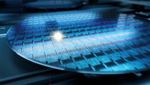
Table of contents
1. What is laser annealing?
2. The advantages of laser annealing in the thermal processing of semiconductors
3. Laser annealing is indispensable in the manufacturing process of power semiconductors
4. The industries where SiC power semiconductors are anticipated to excel
5. Types of light sources used in laser annealing of SiC power semiconductors
6. Product introduction
7. Wrap up
What is laser annealing?
Laser Annealing
Laser annealing is a thermal process used to modify materials, employing a laser beam to locally heat the surface of a wafer or a specific area, followed by rapid cooling. It finds applications in semiconductor and other manufacturing fields for purposes such as activation, alloying, and crystallization.
The advantages of laser annealing in the thermal processing of semiconductors
Advantages of laser annealing
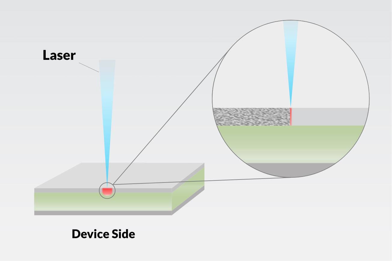
Laser annealing makes it possible to heat only the surface of a wafer, with the advantage of not destroying the device structure. Additionally, the depth of penetration can be controlled by selecting the laser wavelength, allowing for precise control, and enabling treatment of specific areas.
Types of semiconductor heat treatment
There are three main types of heat treatment for semiconductor manufacturing.
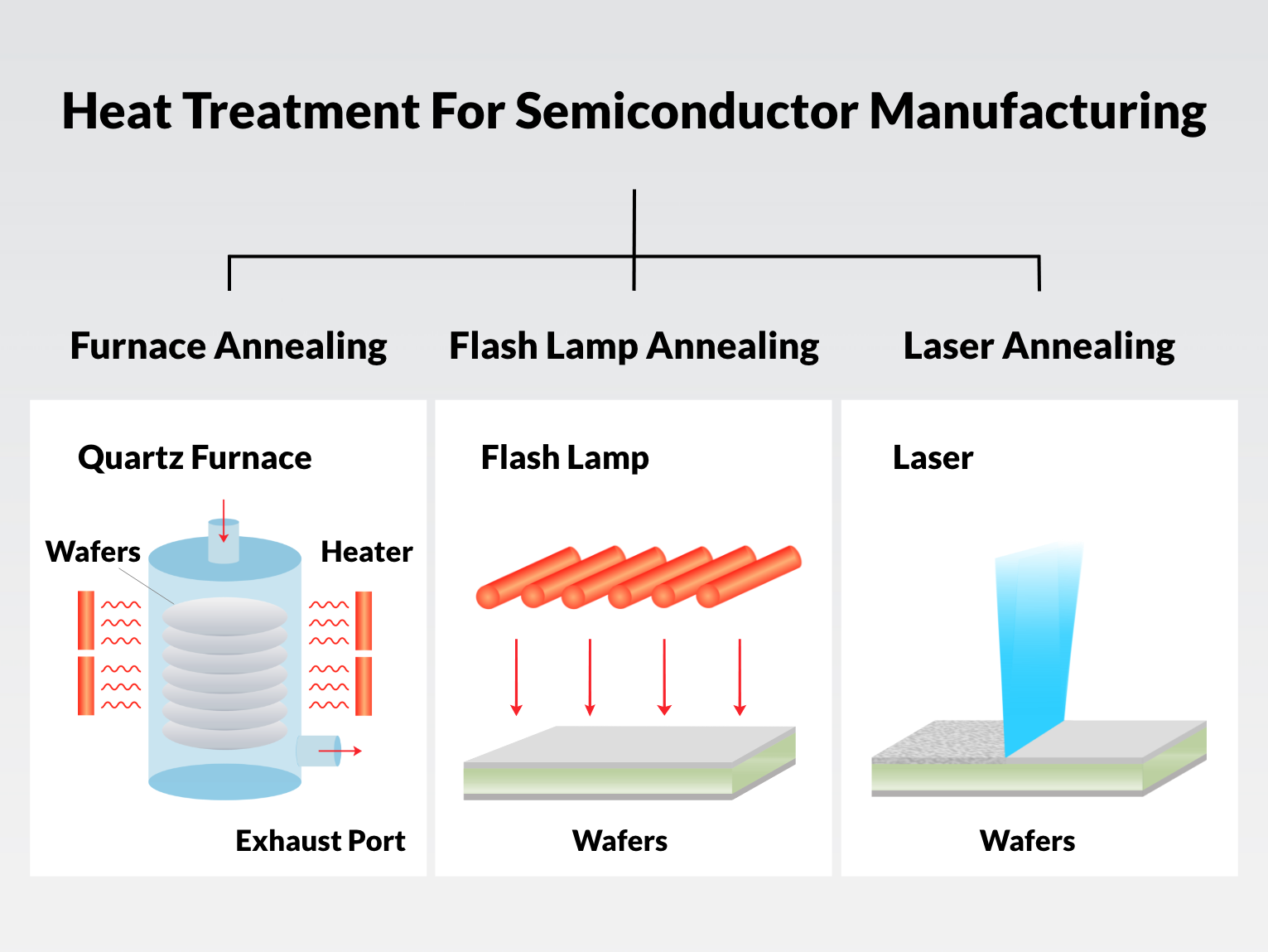
■ Furnace Annealing
This is the method used to heat multiple wafers simultaneously. The wafers are placed inside a quartz core tube and heated externally by a heater.
■ Flash Lamp Annealing
Taking advantage of the characteristics of silicon, which readily absorbs infrared rays, wafers are rapidly heated by emitting infrared flash lamps. The process of rapidly heating wafers is called RTA (Rapid Thermal Anneal).
■ Laser Annealing
This method involves heating wafers by emitting lasers. It is utilized to enhance crystallinity because only the surface layer is melted and can subsequently be recrystallized.
Laser annealing is indispensable in the manufacturing process of power semiconductors
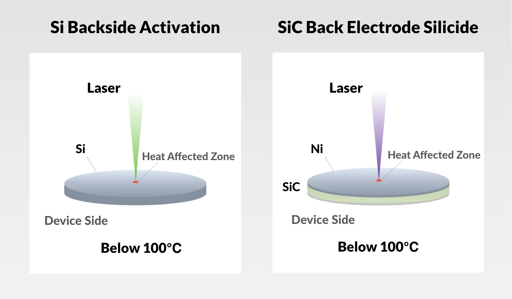
In the manufacturing of power semiconductors, laser annealing processes are widely used for activating impurities doped into the backside of Si-IGBT and for forming silicide (alloying) on the backside metal of SiC-MOSFET.
In both processes, while the temperature of the backside (the side where the laser is irradiated) is raised to about 1000 degrees Celsius, the temperature of the surface (non-irradiated side) where the device structure is formed must be kept below 100 degrees Celsius. Therefore, the laser annealing process, which excels in localized heat treatment, is selected.
For customers considering the introduction of laser annealing equipment
We prepare a test environment by demo systems for the customers to do their process evaluation.
Three types of laser sources are available for testing: IR, Green, and UV wavelengths.
We also provide after-sales service to support for stable equipment operation after installation.


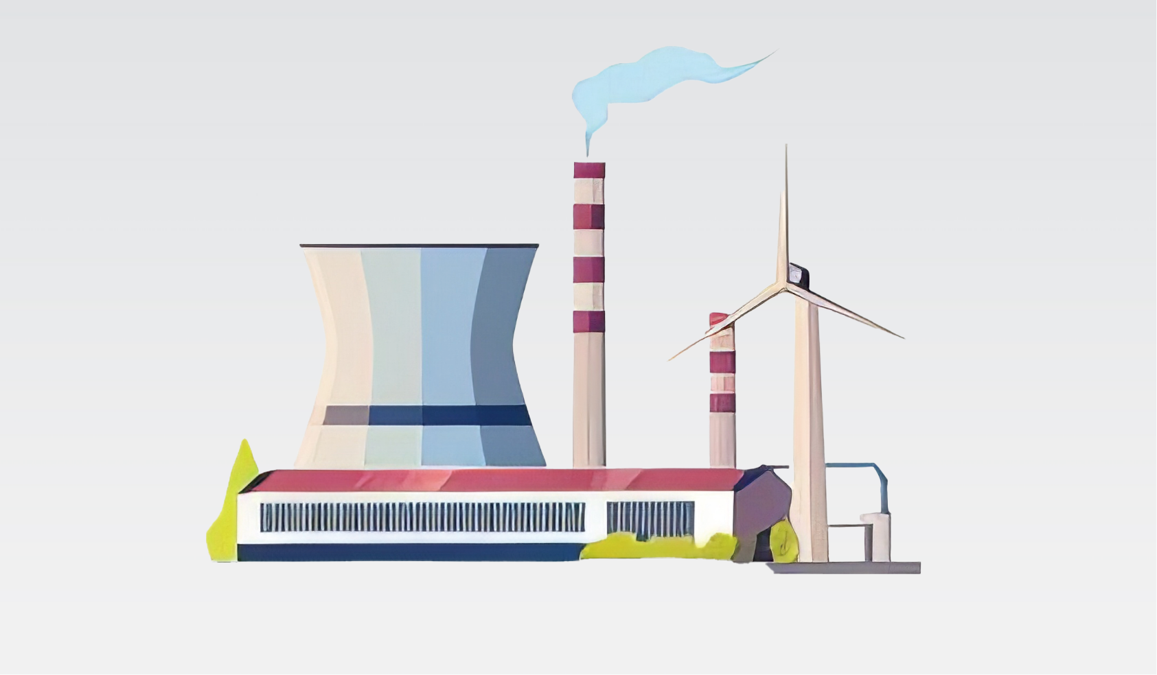
The industries where SiC power semiconductors are anticipated to excel
Amid the recent shift towards a decarbonized society and rising expectations for renewable energy due to energy shortages, SiC power semiconductors are anticipated in industries such as automotive, industrial equipment, railway vehicles, and consumer electronics.
Automotive Industry
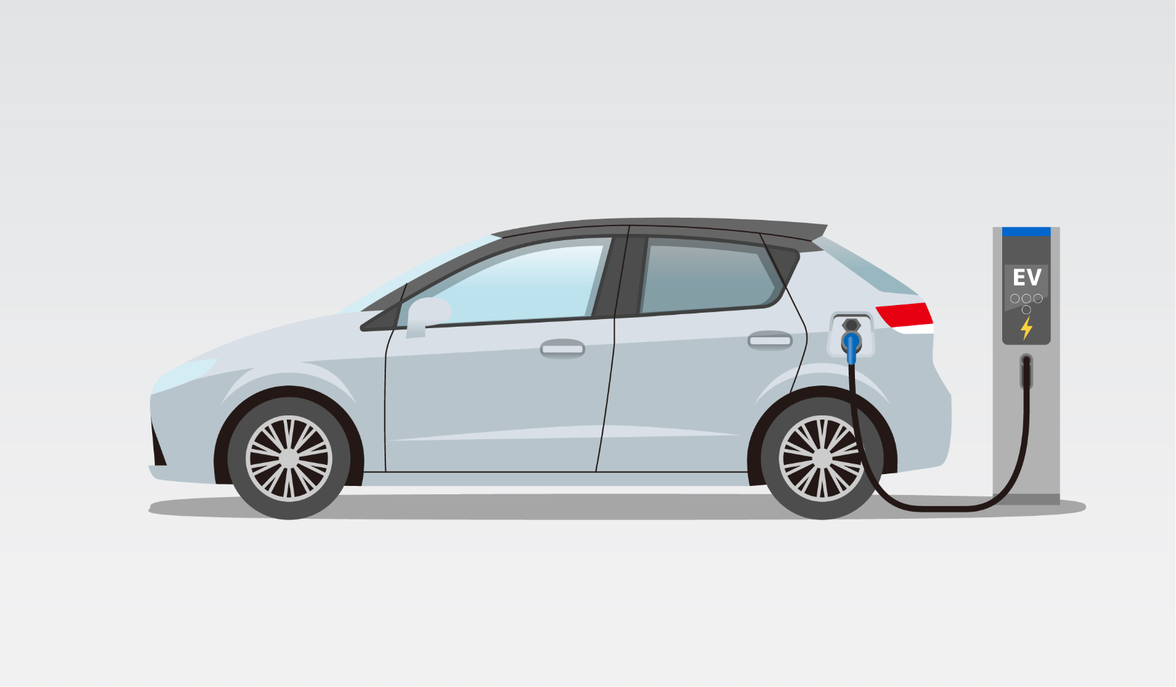
The automotive industry is rapidly promoting the use of electric vehicles (EVs) for decarbonization, leading to an increase in demand for power semiconductors such as Si-IGBTs and SiC-MOSFETs. SiC, in particular, has garnered significant attention due to its wide band gaps, high breakdown voltage, and excellent thermal conductivity.
The main reasons why SiC power semiconductors are important are as follows:
■ High temperature operating performance
EV fast charging handles high current, leading to higher heat generation. SiC power semiconductors have excellent thermal conductivity and resistance to high temperatures, simplifying the peripheral cooling mechanism.
■ High voltage tolerance
Compared with Si, SiC has a higher voltage tolerance, making it possible to use SiC for the drive systems of EVs that operate at high voltages. Especially in recent years, as the demand for fast charging has been increasing, this is one of its most prominent characteristics.
■ Highly efficient power conversion
SiC power semiconductors can be used for efficient power supply in the case of fast charging because they have lower power loss and higher power conversion efficiency compared with existing Si power semiconductors. They also supply power from the battery to the motor more efficiently, enabling longer mileage and higher performance.
Industrial equipment
In the field of industrial equipment, the shift towards a decarbonized society and increasing expectations for renewable energy due to energy shortages are driving the need for improved inverter technologies to promote energy conservation and enhance efficiency.
To achieve higher energy-saving performance and efficiency in inverters, state-of-the-art semiconductors are essential, and the replacement of Si power semiconductors, which are currently mainstream, with SiC power semiconductors is accelerating.
The use of SiC power semiconductors increases the power conversion efficiency of inverters, resulting in reduced power consumption of industrial equipment and energy savings.
Railway vehicle industry
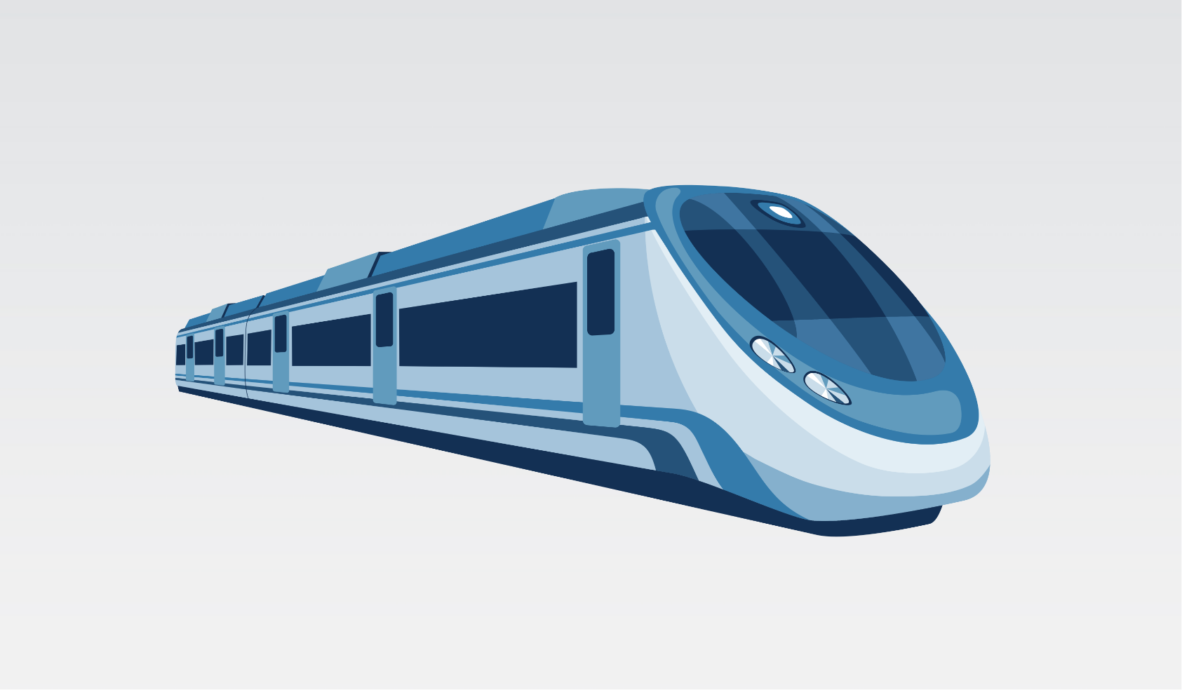
Railway vehicles that utilize high-capacity power electronics require a significant amount of power as they frequently start and stop.
In the case of railway vehicles using conventional Si power semiconductors, a large amount of electricity is generated at high speed, and the power semiconductors cannot withstand the strain. Therefore, mechanical brakes slowed the vehicle down by wasting energy as heat.
However, SiC power semiconductors have attracted attention in recent years for their ability to significantly reduce power consumption by minimizing power loss and greatly improving power regeneration rates. They also have the potential to reduce volume and mass compared to conventional products by streamlining the cooling mechanism due to reduced heat generation.
Home appliances
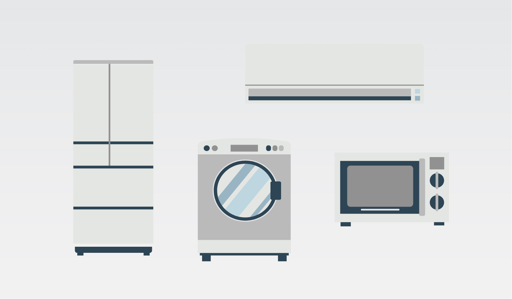
Compared with Si, SiC can lead to significant reductions in power loss due to characteristics such as high temperature operation, fast switching operation, and high heat dissipation. As a result, the adoption of SiC power semiconductors for home appliances such as TVs, air conditioners, refrigerators, computers, and smartphones is also underway.
In addition, due to their characteristics of high voltage tolerance and fast switching operation, they are also effective for products such as microwave ovens and induction heaters where power conversion efficiency is important.
Types of light sources used in laser annealing of SiC power semiconductors
In the process of laser annealing, UV lasers and green lasers are mainly used. Although these laser sources are used for the purpose of activation, alloying, crystallization, etc., differences in wavelengths result in different effects and coverage.
UV laser
UV lasers have short absorption depths due to their short wavelengths and are mainly used in heat treatment processes targeting the top surface layer of the workpiece, such as alloying and crystallization.
Features
The wavelength of UV lasers varies depending on the type of laser oscillator.
■ Third Harmonic YAG Laser
Wavelength: 355nm
YAG lasers are very common lasers, and their third harmonic wavelength is located at 355nm in the UV region.
■ Excimer laser
The wavelength of excimer laser includes below.
Argon Fluoride (ArF) laser: wavelength 193nm
Krypton Fluoride (KrF) laser: wavelength 248nm
Xenon Chloride (XeCl) laser: Wavelength 308nm
Xenon Fluoride (XeF) laser: Wavelength 351nm
Excimer lasers provide higher energy due to their short wavelengths and are utilized for thermal treatment and processing of surfaces, such as annealing and lithography.
Wavelength
■ Absorption in surface layer
The high absorption rate of SiC in the UV wavelength region enables efficient energy absorption near the surface, allowing for localized heat treatment to be performed near the wafer surface.
■ Minimization of thermal effects on the back side
Due to its short wavelength, heat diffusion to the surroundings of the irradiated area is low, resulting in a minimized thermal impact on the back side.
Green laser
Green lasers are utilized for the activation of impurities implanted on the backside of Si wafers or for the crystallization of a-Si. They are suitable for heat treatment targeting deep layers due to their longer wavelength compared to UV lasers.
Features
■ Second Harmonics YAG Laser
wavelength: 532nm
While the basic wavelength of the YAG laser is output at 1064nm, utilizing wavelength-converted optical elements allows for the generation of a second harmonic green laser with a half wavelength (532nm).
Wavelength
■ Moderate penetration depth and uniform heating
The longer wavelength compared to UV lasers enables uniform heating from the surface of the workpiece to a certain depth, making it effective for uniformly improving the characteristics throughout the material.
■ Proper management of thermal effects
It's easier to obtain higher energy power than UV lasers and can be processed in a faster time. A shorter processing time reduces the impact of thermal effects due to thermal conduction.
Product introduction
SHI has been focusing on and developing laser annealing processes before power devices became a key device for realizing a low-carbon society. Since the delivery of the first unit in 2004, more than 150 systems have been supplied worldwide, supporting the production of various device manufacturers.
We are committed to contributing to the development of markets with growth potential and to the realization of a decarbonized society by continuing to supply high-performance laser annealing devices moving forward.
SWA “Green/Hybrid” Laser series
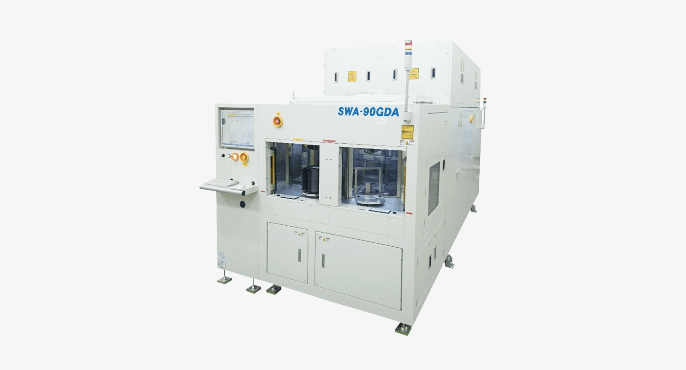
SWA “Green/Hybrid” Laser series
High-performance laser annealing devices for deep activation and double-pulse processes
Application examples: Backside activation of IGBTs
These are hybrid annealing devices equipped with solid-state and long-wavelength lasers that enable a unique double-pulse process. They feature solid-state lasers, including high repeated pulse energy stability, maintenance-free operation, and compact design, promoting the development of next-generation processes in the semiconductor field.
> Click here for detail
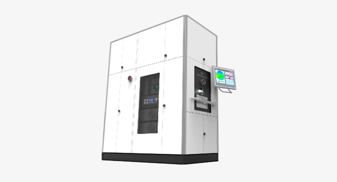
SWA “UV” Laser series
SWA “UV” Laser series
Laser annealing devices for the next-generation power devices
Application examples: SiC ohmic contact generation, activation, etc.
The metal-SiC interface is heated to high temperature while suppressing the temperature raise of the non-irradiated surface, and OPTSWING (proprietary high-speed scanning method) realizes the generation of ohmic contacts.
> Click here for detail
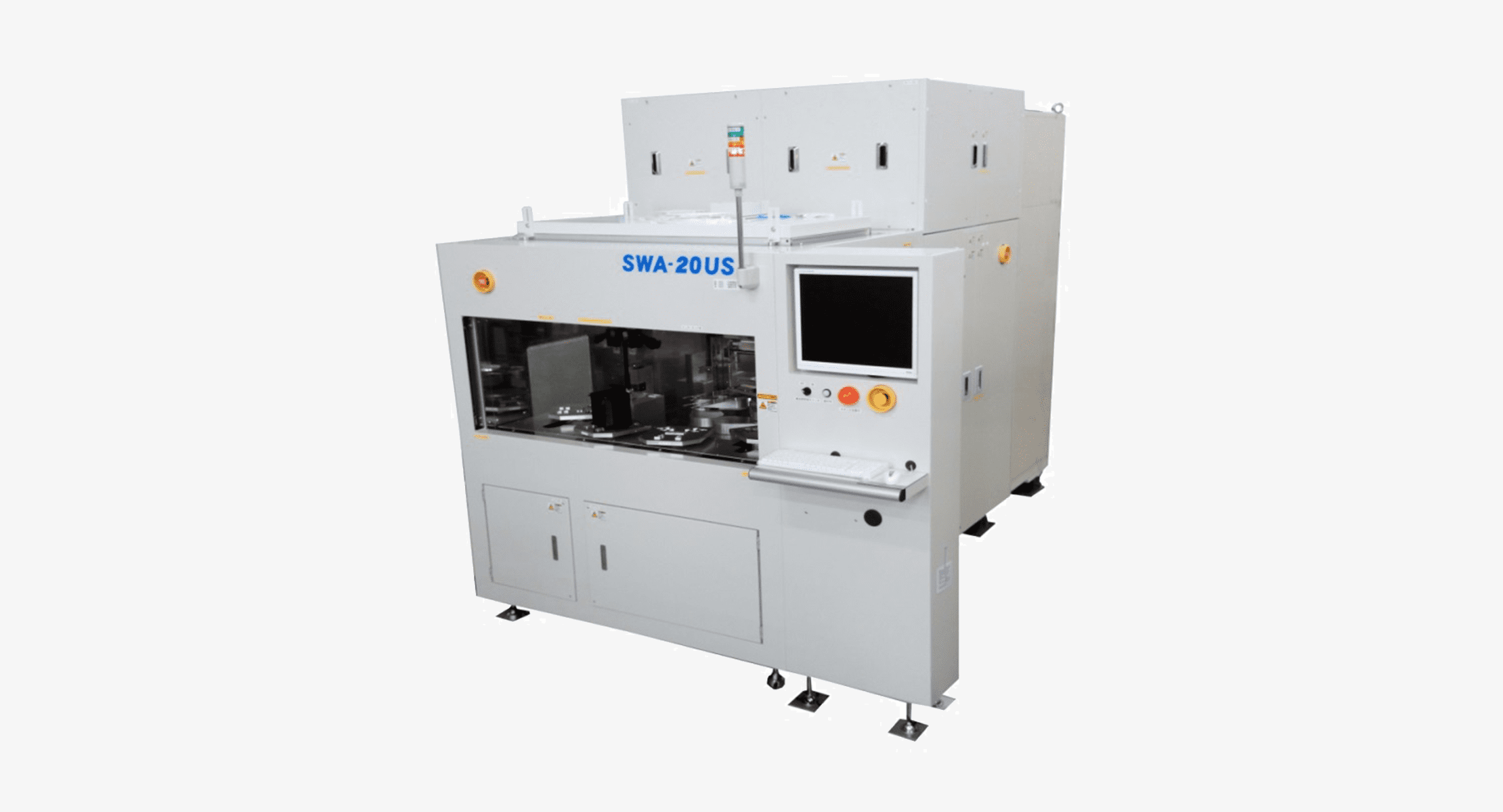
SWA “UV” Laser series for R&D
SWA “UV” Laser series for R&D
Versatile manual system device equipped with the optical system of SWA-20US, which has an extensive track record in mass production.
Application examples: SiC ohmic contact generation, activation, etc.
Manual system suitable for development and small volume productions
It features a UV laser + OPTSWING (high-speed scanning) + process chamber mounted for high-quality processes.
*For inquiries about light sources other than UV lasers, please consult us separately.
> Click here for detail
Wrap up
How do you find it? Laser annealing is one of the technologies utilized in the process of the development of semiconductors and the necessary process for the development of semiconductors towards decarbonized society in recent years.
Please feel free to contact us if you have any concerns about laser annealing or if you are considering introducing it to your company.
For customers considering the introduction of laser annealing equipment
We prepare a test environment by demo systems for the customers to do their process evaluation.
Three types of laser sources are available for testing: IR, Green, and UV wavelengths.
We also provide after-sales service to support for stable equipment operation after installation.