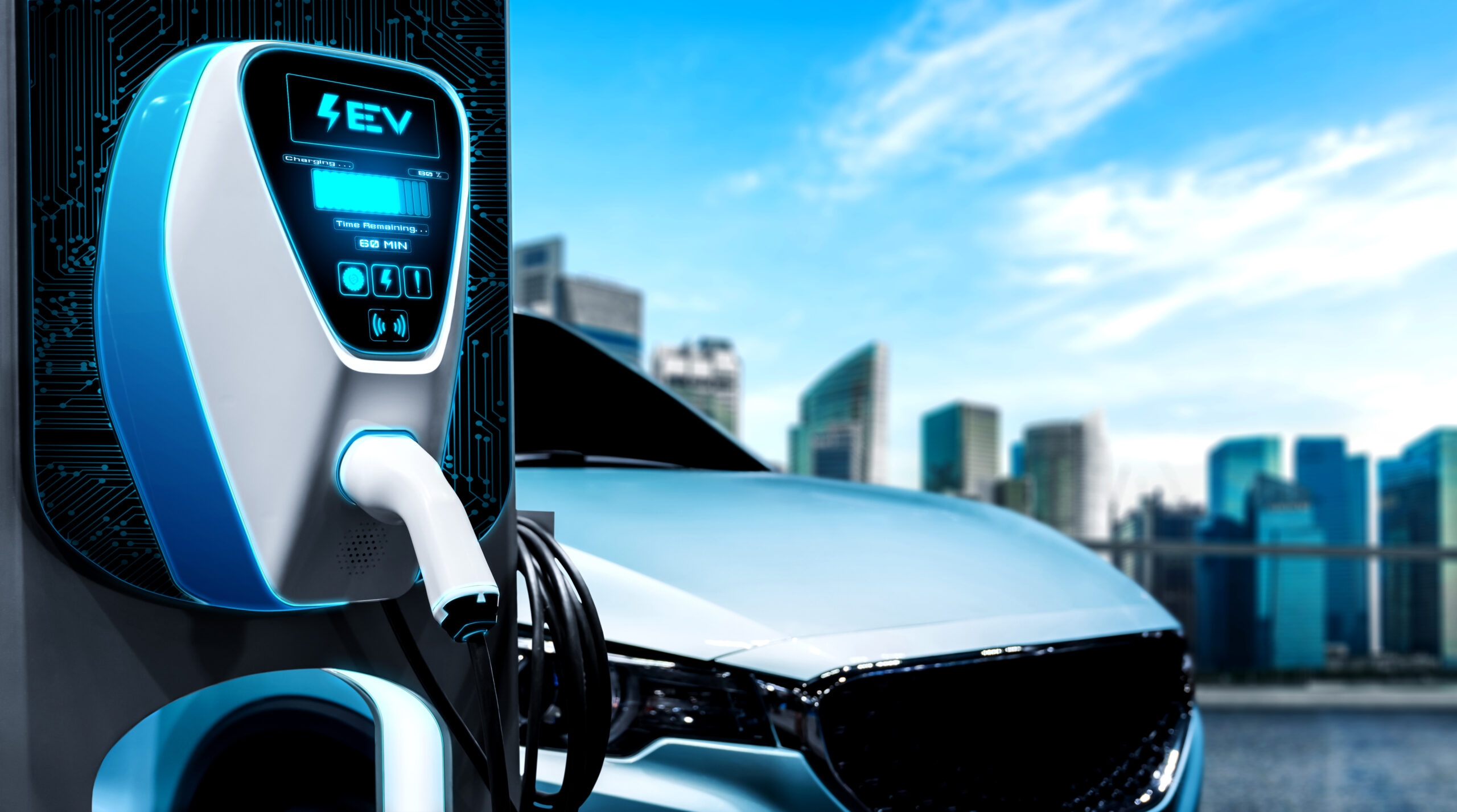
Currently, the world is moving toward decarbonization in order to solve the climate change problems. In the automotive industry, it is said that EV(electrical vehicles) are essential and SiC power device, which have higher voltage resistance than Si, are attracting attention. As a leading manufacturer of laser annealing system, SHI are contributing to a decarbonized society.
SOLUTION
Laser Annealing
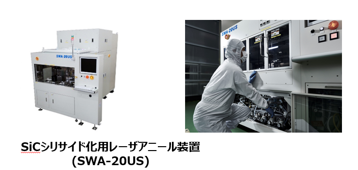
Contributing to a decarbonized society with laser annealing system for SiC power device that is essential for EV
Global issues
- For a decarbonized society, the development of EVs is essential in the automotive industry.
And, SiC, which better energy loss than Si, are attracting attention
- SiC device makers aim build mass production and supply system as soon as possible
Solutions
- Laser annealing system contribute to production of SiC power device in the world, where SiC and metal are alloyed to reduce electrical resistance.
Why SiC power decvices are required for EVs
SiC has the following advantages to Si
・ Low resistance: The impurity concentration can be higher than Si, so making thinner drift layer is possible. As a result of that, high-withstand-voltage
devices with lower on-resistance can be realized.
・ High-speed operation: Fast operating devices such as SBDs and MOSFETs can be used with maintaining high-withstand-voltages.
・ High temperature operation: SiC’s band gap is approximately 3 times wider than Si, device operation during higher temperatures is possible.
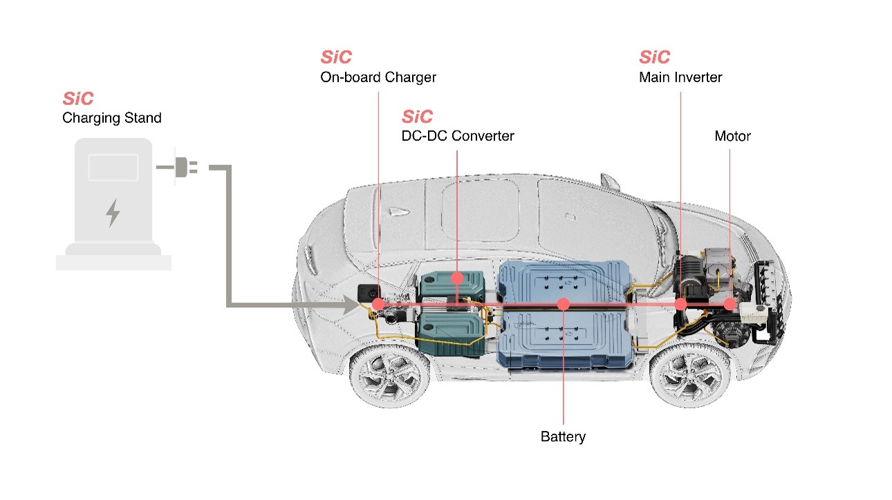
SiC power semiconductors used in various units in EV
Why is laser annealing process necessary for SiC power semiconductor manufacturing?
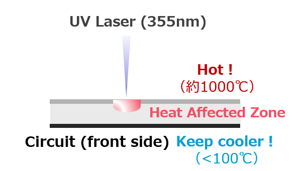
Silicide: Laser annealing system is used in the silicide process of SiC power device to improve electrical resistance by alloying SiC and metal on the backside of the wafer. In this process, the temperature of the wafer backside (laser irradiated side) must be increased to apx.1000°C, while the wafer front side (non-irradiated side) where circuits are formed must be kept below 100°C. The laser annealing process can achieve this process due to partial heat process.
Sales record for SiC power device process
SHI has been selling laser annealing systems for SiC silicide process since 10 years ago when SiC production first started in the market. Since our first system was installed in 2013, we have sold more than 70 systems in the world, contributing the production of various SiC device customers. By continuing to supply high-quality laser annealing systems, we will keep contributing to the market and to a decarbonized society.